
From the silicon chips powering smartphones to the gallium nitride transistors in an electric vehicle, it’s all about the material choice. The material can determine many factors in the semiconductor’s success, such as the device’s speed, power efficiency, heat management, reliability, and future scalability. How does the material choice affect all of these factors?
In this blog post, we will take a look at the effect materials have on a semiconductor’s performance and how to choose the right material for your project.
How do material properties shape device performance?
Materials for semiconductors are not all equal. Intrinsic properties, such as bandgap, electron mobility, thermal conductivity, and breakdown voltage, can directly affect a device’s capabilities.
The following table weighs some of these factors with a few different materials:
| Material | Bandgap (eV) | Electron Mobility (cm2/V•s) | Thermal Conductivity (W/m•K) | Breakdown Voltage (MV/cm) | Key Strengths |
|---|---|---|---|---|---|
|
Silicon (Si) |
1.12 |
1400-1500 |
150 |
0.3 |
Cost Maturity |
|
Gallium Arsenide (GaAs) |
1.42 |
8000 |
46 |
Moderate |
High Speed Radio Frequency |
|
Silicon Carbide (SiC) |
3.2-3.26 |
650-900 |
490 |
3.0 |
Power Efficiency Heat Management |
|
Gallium Nitride (GaN) |
3.2-3.4 |
990-2000 |
130 |
3.3-3.5 |
Power Efficiency Radio Frequency |
Key Properties:
- Bandgap: Voltage and temperature limits. For example, a wide bandgap means high power/high temperature.
- Electron Mobility: The higher the mobility number, the faster the electrons can switch, and the higher the frequency at which the electrons move throughout the material with the application of an electric field.
- Thermal Conductivity: Better heat dissipation means a higher reliability and power density.
- Breakdown Voltage: The higher the value, the greater the ability to withstand higher voltages without failure.
Food for Thought:
The wide bandgap in materials such as SiC and GaN is revolutionizing power electronics and radio-frequency applications. Silicon remains dominant for general-purpose logic due to its cost and process maturity.
Speed, Power, Heat, and Reliability Performance Impacts for Semiconductor Materials
- Speed and Frequency
- High-Mobility Materials: Gallium arsenide and gallium nitride enable ultrafast electron switching, which is important for radio-frequency, 5G, and high-speed computing.
- Silicon: It is a sufficient material for most digital logic, but can be outpaced in high-frequency domains.
- Power Efficiency
- Silicon Carbide and Gallium Arsenide: These materials enable devices to operate at higher voltages and frequencies with lower losses. They are ideal for power conversion and electric vehicles.
- Advanced Architectures: Fin Field-Effect Transistors (FinFETs) and Gate-All-Around (GAA), when paired with the right material, can further reduce power consumption.
- Heat Dissipation
- Silicon Carbide and Diamond: Both materials excel at heat dissipation while supporting higher power densities and reliability.
- Thermal Management: It is a limiting factor in dense, high-performance chips. Material choice is the first line of defense when it comes to this property.
- Reliability and Lifespan
- Inorganic Semiconductors: Silicon, silicon carbide, and gallium nitride can perform well under stress, ensuring long device lifespans.
- Material Purity and Defect Density: Critical in advancing processing and passivation techniques, and are used to minimize failures.
How do leading manufacturers choose materials for semiconductors?
Application-Driven Selection
| Domain | Preferred Materials | Selection Criteria | Example Applications |
|---|---|---|---|
|
CPUs and GPUs |
Silicon Silicon-Germanium (SiGe) High-k (Hafnium Dioxide and Zirconium Dioxide) |
Mobility Scalability Process Compatibility |
PCs Server Processors |
|
Memory Devices |
Silicon Chalcogenides |
Retention Endurance Integration |
DRAM NAND PCM |
|
Power Electronics |
Silicon Carbide (SiC) Gallium Nitride (GaN) |
Wide Bandgap Thermal Stability |
EV Inverters Industrial Drives |
|
Radio Frequency Applications |
Gallium Arsenide (GaAs) Indium Phosphide (InP) Gallium Nitride (GaN) |
High Frequency Low Noise |
5G Base Stations Satellite Comms |
Decision Factors
- Mission Profile: Speed, power, temperature, and expected lifetime.
- Integration: Compatibility with existing process flows and ability to co-integrate materials.
- Cost and Supply Chain: Availability and maturity of high-purity materials.
Food for Thought:
Many factors should go into the material decision for your project. It’s not just about the physics, but manufacturability, cost, and integration with existing technologies also need to be considered.
Emerging Semiconductor Materials and Technologies
2D Materials and Compound Semiconductors
- 2D Materials: Molybdenum disulfide (MoS₂) and tungsten diselenide (WSe₂) enable ultimate scaling and ultra-thin channels, as well as new device architectures, GAA, and CFET.
- Compound Semiconductors: GaN and InP push the limits in high-frequency, high-power, and optoelectronic applications.
- Novel Substrates: Engineered substrates, such as Gallium Nitride on Trap-Rich Silicon-On-Insulator (GaN-on-TRSOI) and layer transfer techniques, are enabling new integration schemes.
- Challenges:
- Achieving large-area, defect-free films.
- Forming low-resistance contacts and reliable gate stacks.
- Scaling up manufacturing to match silicon’s cost and yield.
Visualizing the Impact
Performance Trade-Offs by Material Systems
| Material and System | Speed | Power Efficiency | Heat Dissipation | Reliability | Applications |
|---|---|---|---|---|---|
|
Silicon (Si) |
Moderate |
Good |
Moderate |
High |
CPUs General ICs |
|
Silicon Carbide (SiC) |
High |
Excellent |
Excellent |
Very High |
Power Electronics EVs |
|
Gallium Nitride (GaN) |
Very High |
Excellent |
Good |
High |
Radio Frequency High-Frequency Power Devices |
|
2D Materials (MoS2) |
Very High |
Excellent |
Good |
Good |
Ultra-Scaled Flexible Electronics |
|
Organic Semiconductors |
Low |
Moderate |
Poor |
Low |
Flexible/Wearable Devices |
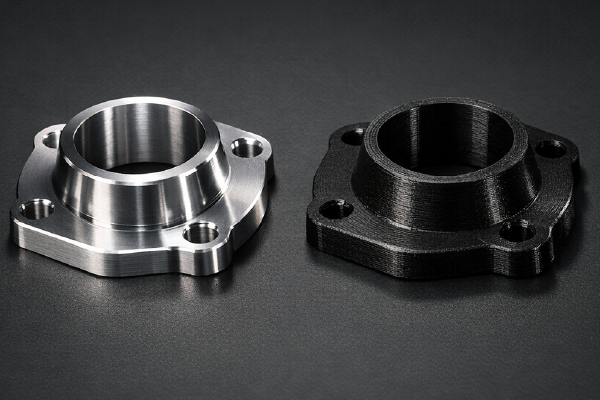
Manufacturing semiconductors with Prototek Digital Manufacturing.
3D Printing
- Applications: Prototypes of machined parts, jigs, fixtures, and housings for semiconductor equipment.
- Advantages: Speed, flexibility, and the ability to create complex shapes.
CNC Machining
- Applications: Wafer chucks, gas distribution plates, machine frames, and custom tooling.
- Materials: High-purity plastics, silicon, aluminum nitride, and specialty metals.
Sheet Metal Fabrication
- Applications: Integrated circuits (ICs) on silicon wafers and housings.
Molding and Casting
- Applications: Mass-producing plastic parts for equipment, protective covers, supports, and custom enclosures.
- Materials: High-purity plastics and specialty polymers to avoid contamination.
FAQs
Semiconductor materials are essential for electronic devices, enabling the control of electrical currents.
The following materials are examples of semiconductor materials: silicon, gallium arsenide, indium phosphide, germanium, silicon carbide, and gallium nitride.
The energy gap between the valence and conduction bands. This gap can determine a material’s electrical properties. Conductors have no gap, while semiconductors have a small gap, and insulators have a large gap.
Advanced semiconductor architectures enable higher performance, efficiency, and integration through innovative designs and technologies.
Organic semiconductor materials, such as carbon-based materials, can be flexible, low-cost, and processed at lower temperatures. They offer advantages for flexible electronics, for example, OLEDs and solar cells. They perform worse than inorganic semiconductors.
Inorganic semiconductors, such as silicon and gallium arsenide, are rigid and high-performing but can be energy-intensive to produce, making them more costly and environmentally challenging to create.
A wide range of applications use semiconductors, including smartphones, computers, automotive electronics, renewable energy systems, and medical devices.